
RF PCB Be Used in Automotive Applications
RF PCBs facilitate wireless transmission and reception of data or control signals modulated onto a high-frequency carrier wave. These boards are used in a wide variety of applications like wireless connectivity, radar, navigation, IoT and automation devices. They can be fabricated on rigid or flex laminates. They feature controlled impedance typically around 50 or 75 ohm, advanced substrate materials with a low loss tangent and design flexibility that enables seamless integration of passive and active components. They also offer shielding structures like ground planes and guard traces that reduce crosstalk, ensuring signal integrity.
With increasing electronics content in automobiles, demand for infotainment, electrification and autonomous features are driving rapid growth in rf pcb designs. To meet the requirements of these complex designs, designers must master signal integrity, robust power distribution, thermal management and quality/reliability validation. This requires innovations in PCB materials, high-density integration and panel scale manufacturing.
The choice of a circuit board material is a critical factor in the performance of any electronic device, especially an automotive one. PCBs that are destined for use in a vehicle are exposed to a range of harsh conditions, including extreme temperatures, high pressure and corrosive environments. Moreover, they must withstand vibrations and abrasions, while maintaining high reliability over a 10-year life expectancy.
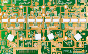
Can RF PCB Be Used in Automotive Applications?
To meet these challenges, the RF PCB needs to be designed and manufactured using specific materials that can handle high-frequency signals and deliver exceptional durability. The typical PCB design consists of several layers, with copper traces that connect different components via vias. In order to ensure high signal performance, the traces must be properly routed and impedance-matched. This is possible by minimizing trace lengths, differential signaling and isolating analog and digital signals. Additionally, proper supply decoupling is essential for preventing noise and interference.
Moreover, the RF PCB must be able to handle the power required for transmitting these signals over long distances. This can be achieved by using a specialized substrate material, such as PTFE (polytetrafluoroethylene). It has high dielectric constants and is characterized by very low losses, making it an excellent choice for high-frequency PCBs. In addition, this material is compatible with standard PCB drilling techniques and can be used for both rigid and flex circuits.
Moreover, RF PCBs are often subjected to stringent EMI/EMC (Electromagnetic Interference/Electromagnetic Compatibility) requirements to ensure compliance with regulatory standards and prevent interference with other electronic devices. RF PCB manufacturers employ various EMI mitigation techniques such as shielding, filtering, and layout optimization to suppress unwanted electromagnetic emissions and enhance the overall EMC performance of RF systems.
Lastly, the RF PCB must be characterized for its conductive properties and mechanical strength. This can be accomplished by performing a series of tests on the finished product, such as automated optical inspection, X-ray inspection and electrical testing using Time-Domain Reflectometry (TDR) to verify that the board performs as intended. It is also important to consider the environmental and reliability standards that the RF circuit board must meet before purchasing it. These can be found in industry publications such as IPC-A-610G Automotive Addendum and AEC-Q100.