
HDI PCBs on Product Reliability
The quality of printed circuit boards is a crucial factor in determining the reliability and performance of electronic products. High-Density Interconnect (HDI) PCBs are a significant advance in the technology, packing more functionality into smaller boards and allowing for more compact and lightweight equipment. In this article, PCBSky explores how choosing the right HDI PCB supplier can make your product more reliable and competitive.
The use of micro lines and highly compact layouts allows designers to place components much closer together, which reduces the number of layers needed for a circuit board and improves its electrical conductivity. Additionally, the elimination of stubs and shortening of signal paths improves signal integrity by reducing electromagnetic interference and power noise.
A high-density PCB’s structure enables it to be made from thinner materials, which further reduces the weight and size of the device. This is especially beneficial for wearable devices, which need to be slim and lightweight, but also feature-rich to enable advanced connectivity and performance.
Increasingly popular with consumers, wearables are used for everything from health tracking to GPS and wireless communication. To meet this demand for sleek, powerful gadgets that can be worn on the go, hdi printed circuit boards are key.
The technology is also used in medical devices, where high-performance and precision are essential. Whether it’s in patient monitoring systems or surgical equipment, HDI technology provides the necessary reliability to make sure these vital devices can be used safely and effectively.
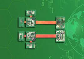
The Impact of HDI PCBs on Product Reliability
Due to the reduced footprint and thinner materials, HDI PCBs are more cost-effective than traditional PCBs. They also require fewer layers and can be made with a lower pitch, which saves on space and material costs. Additionally, HDI PCBs utilize a variety of techniques to streamline the manufacturing process, such as reducing the number of sequential laminations with via-in-pad and blind via technologies.
Moreover, the use of HDI PCBs can help manufacturers save time and money by cutting down on testing and inspection times. This is because the shorter signal paths and the high-density interconnection design allow for a more efficient test and inspection process. HDI PCBs often include buried or blind vias, which are vias that do not go through the entire board, further enhancing design flexibility and reducing size. These features allow HDI PCBs to be thinner, lighter, and capable of handling higher speeds and frequencies, making them a preferred choice for high-performance electronic devices.
With such a wide range of benefits, HDI PCBs have become an integral part of today’s advanced electronics. But the success of any project depends on choosing the right supplier for the job. Choosing an experienced and reputable provider can help ensure that your project is completed on time and within budget, while providing you with the highest quality circuit board available. To learn more about what it takes to choose the best HDI PCB supplier for your product, contact the experts at Netvia Group. We can guide you through the process of designing and assembling an effective PCB that meets all of your specifications. We can also provide you with a quote for your next project.